Switch to full layout
Force Russian
Main shit - the best the newest and the most realistic - all about DtZ !
:> My computers: Z80,68K, etc
:> 68008 SBC AVR (atmega8) Booted minimal computer by DtZ with serial port MC68008 :> 68K 16 bit 68EC000 + Atmega16 computer, epoch III - again booted with AVR with direct memory initialization
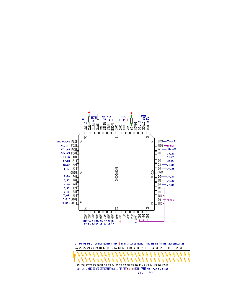
68EC000 Computer by DtZ
"Понесла'сь пизда' по ко'чкам"
Russian proverb, means "Things are up and running"
THIS DOCUMENT IS JUST STARTED!
20150101
So I have a good working 8 bit computer out of 32bit CPU with ISA bus. And
I have Z8001, NS32016 and 16 bit-data-bus version of i960 CPUs. Also I want to use
some more PC hardware, mostly ISA-16
I have a CPU card, with a 8-16 bit switch. So the next will be an 16 bit "motherboard",
well, main board, that will be plugged in the same backplane
Sure I'll use 40 pin ATMega - that will be ATMega16 instead of 28 pin Atmega8,
just because I'm going to use 16 pin as a data bus.
Next, remembering that 20 Mhz 68EC000 refuses to work on low freqs at all (and scince I
have 16 bit data bus) I'll install Address Bus latches and change the booting scheme.
Instead of "feeding" CPU durung initial load, I'll transfer initial program to RAM,directly
accessing it,and then run CPU at full speed, and that is SIGNIFICANT CHANGE from
8 bit project refered as Epoch I and Epoch II
I start with 68EC000, because I allready have this board soldered (and well, 68000 will go,
68HC001, etc, etc, 68010 even, but I'm not sure)
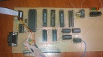
20160404 Fotos
20160315
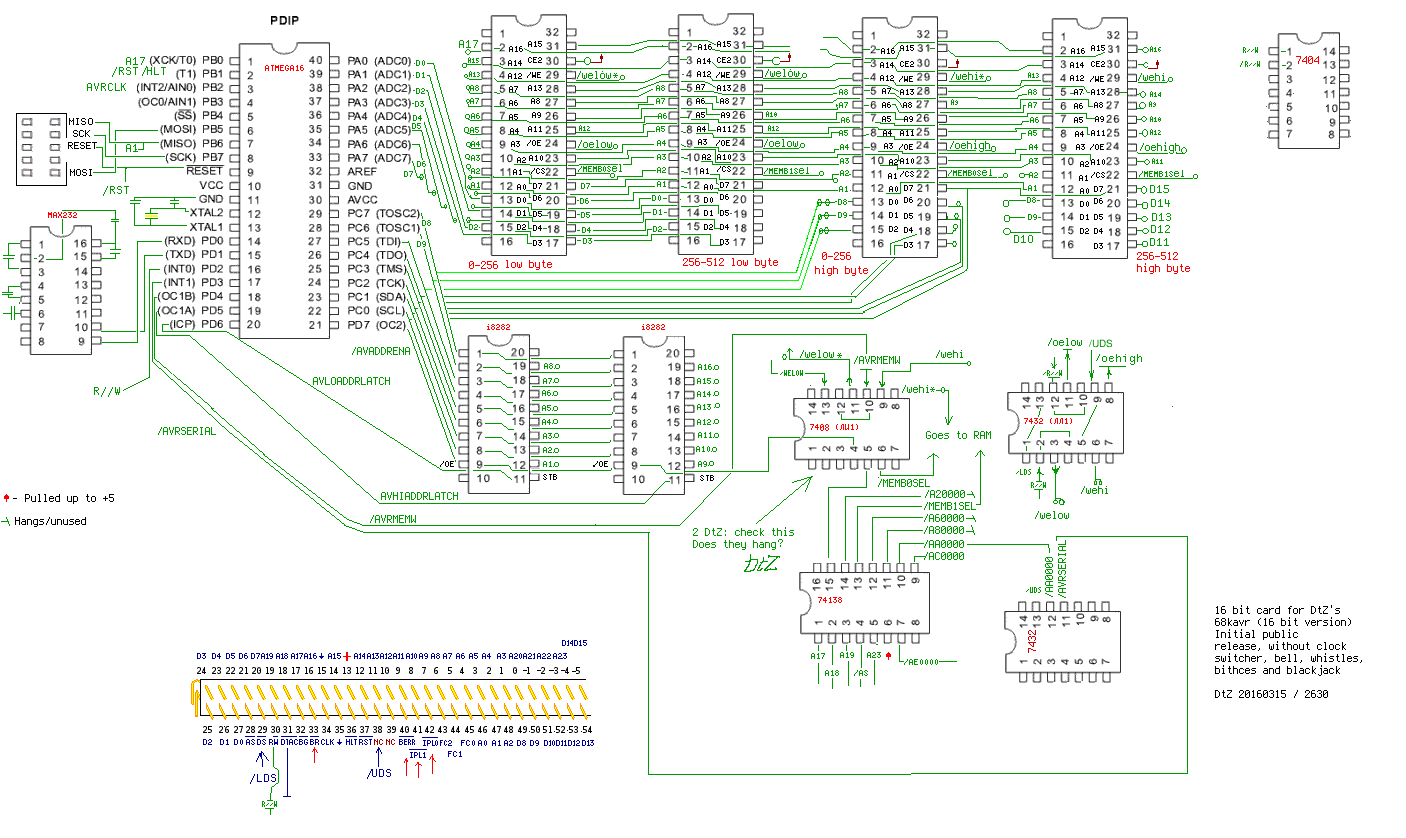
And here is the initial scheme. I really wanted to
keep it small, but it hardly fits to the screen! (but, really, it's larger then 8 bit version because of
address latches and 4 RAM chip from the start; also, note that CPU is on the separate board)
But, before talking about it, lets' see the CPU board from Epoch II.
See the Mode on pin 19? We have to install a jumper there, called 8BIT/16BIT. And for the 16 bit
operation it should be tied to +5.
Also, we have to solder A8-A15 (pins 48-54 and pins -5, -4) and UDS pins to the socket (pin 38)
Lets start with ATmega16. Ports A and C are data bus (and note that port C is wrong ordered, bit 7
of port C goes to bit 8 of data bus, bit 0 to bit 15 of data bus; that's mostly a error, but I've
already soldered this way)
Also, port C is a address bus and goes to latches. But wait! What's THAT? What's the i8282? Where have
I stollen them?
You are almost right. That are the SOVIET KR580IR82 chips. They are the Soviet legacy, we have
a tonns of them here. Normally they should be changed to some 8 bit registers; we'll discuss it later.
To write a byte to the memory (I have only first and third RAM chip installed currenly, 256K totally,
but as you can see place for 512K is reserved), it has to:
- Well, we keep CPU halted. PB1/Pin 2 (Reset+Halt) is low and PB2/Pin 3 (AVRCLK) clicks diring this operation - just CPU to
initialise diring this operation
- /AVADDENA Pin 21 is initialy high, so address latches does not output anything, and
A17, Pin 1 is in high impedance state
- MCU puts A1-A8 values to Port C
- It latches it playing with AVLOADDRLATCH, Pin 20 to the left i8282
- MCU puts A9-A16 values to Port C
- It latches it playing with AVHIADDRLATCH, Pin 19 to the right i8282
- It sets A17, Pin 1, which goes directly to CPU A17 bus.
- It displays data both to Port C and Port A. (prevously rotates Port C data because
of error mentioned in the beginning of this chapter)
- It enables output from the latches to address bus, playing /AVADDENA Pin 21 (and is
mixed by 7808 (ANDed) with /A00000 output from the 74138 decoder)
- Then it drives /AVRMEMW Pin 18 low. It is mixed (ANDed) with /UDS+R//W (called /WELOW)
and /LDS+R//W (called /WEHI) on the 7808 chip, thus making /WELOW* and /WEHI* signals
- In this moment data goes to memory
- Then it drives /AVRMEMW to High
- It drives output off the latches playing /AVADDENA Pin 21
- It takes A17, Pin 1 to the high impedance state
With this simple procedure the initial program transfers to the memory
Then, it takes Pin 2 (Reset+Halt) pin to high and continue clicking Pin 3 AVRCLK in a loop.
When CPU starts, it puts the address on address bus, it is decoded by 74138. PIN 15 of 138 is
mixed with /AVADDRENA as I explained. The /WELOW and /WEHI signals are, as I said, /UDS+R//W and /LDS+R//W,
ORed on 7432; the same thing with /OELOW and /OEHIGH, but instead of R//W, the inverted R//W, called /R//W
signal, taken from 7404 pin 2 is used. And there is no need to mix them with MCU output, because MCU does
not read memory.
Sure we use MCU as UART. So /AA000 signal from 74138 is ORed with /UDS and goes as /AVRSERIAL
to Pin 17 of MCU, thus making an interrupt. Pin 16 is listening to R//W line and Pin 7 is listening at A1
to determine what it actually reads or writes.
Pins 6-9 of MCU is a regular AVRISP (or like that) socket for AVR programming, and Pins 14-15
are normal UART with no RTS/CTS at this moment.
And, well, CPU runs my unmodified firmware from Epoch I/Epoch II!
20160403 And here are the project files
Main Board with bells and whistles
20171225
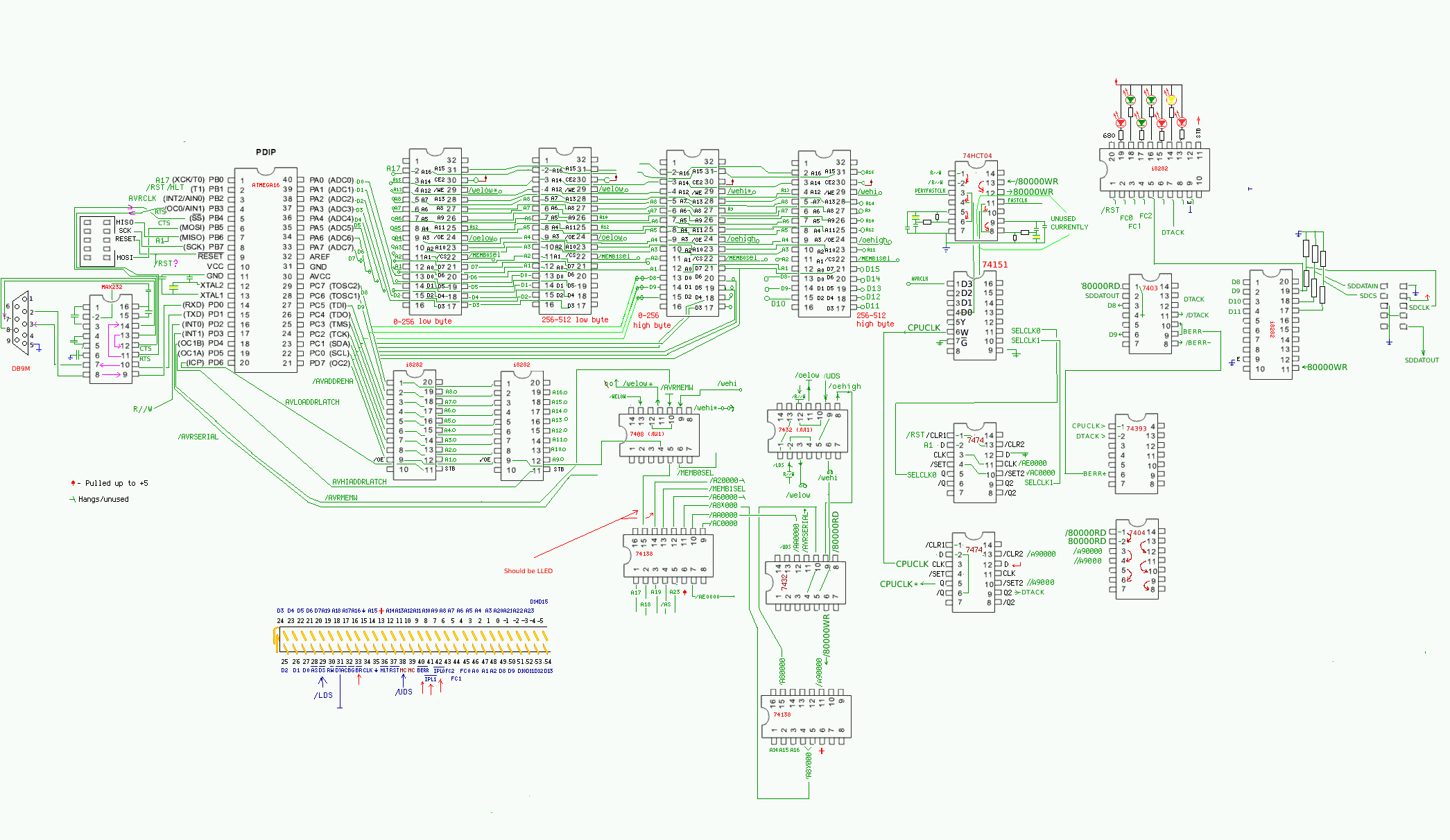
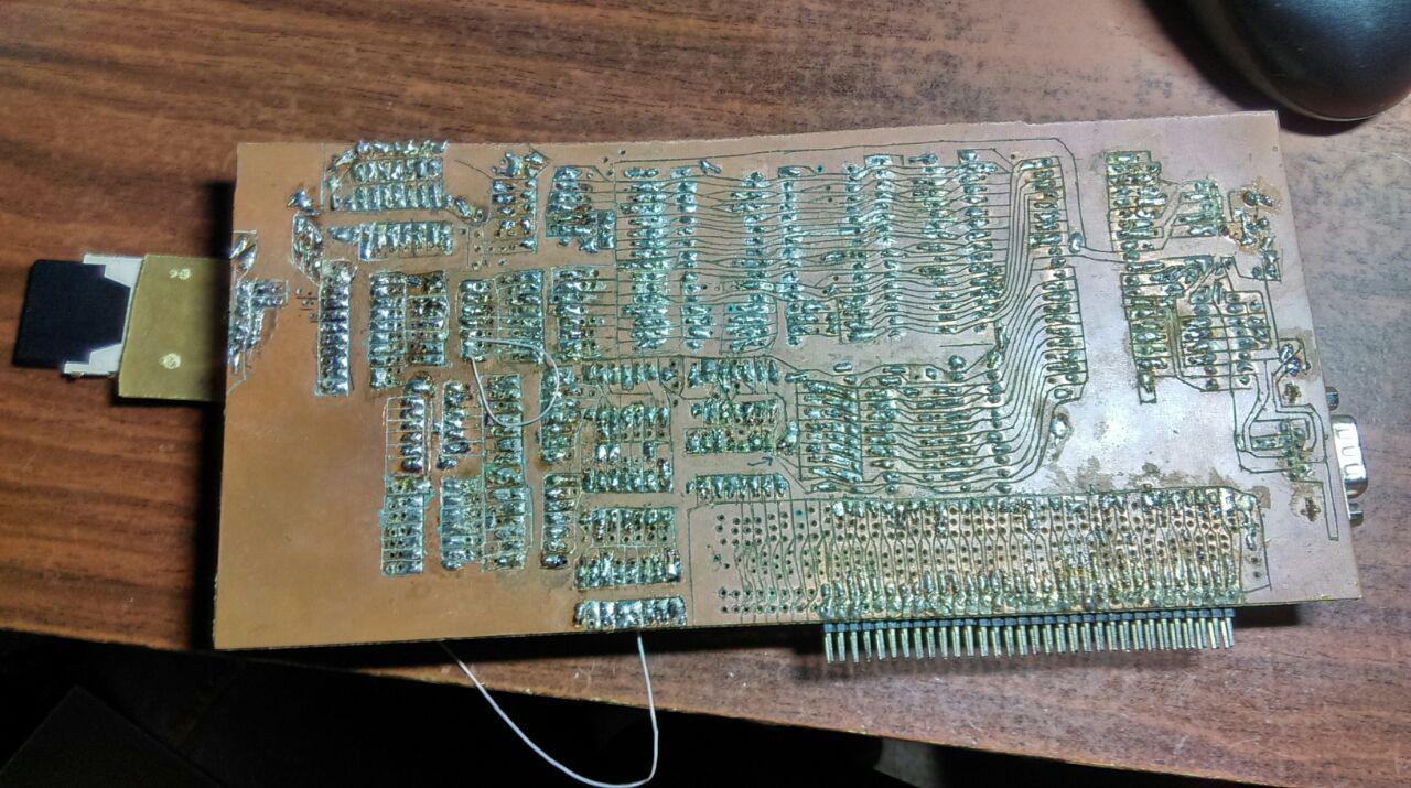
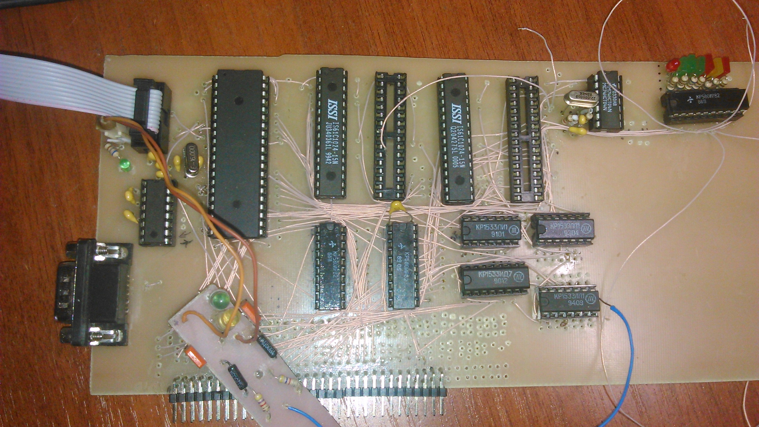
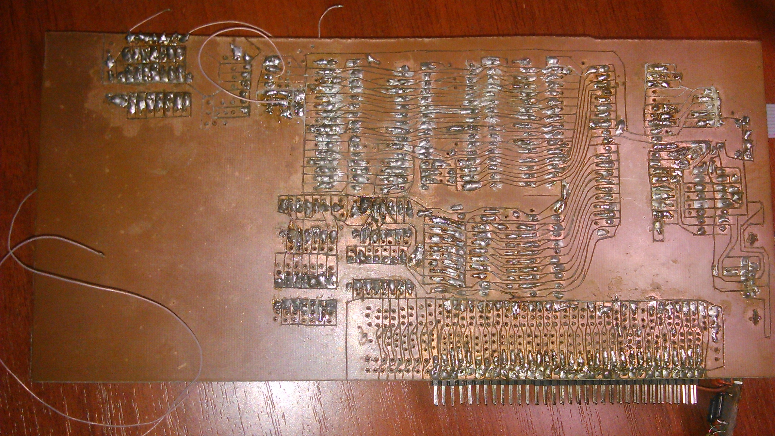
Well, know what? I run the board for almost a year with 256K RAM and almost forgot what is where!
So there should be a new full scheme
..and fotos (yes, the board is ugly as hell, but it works, and to keep it working I'm writing all this)..
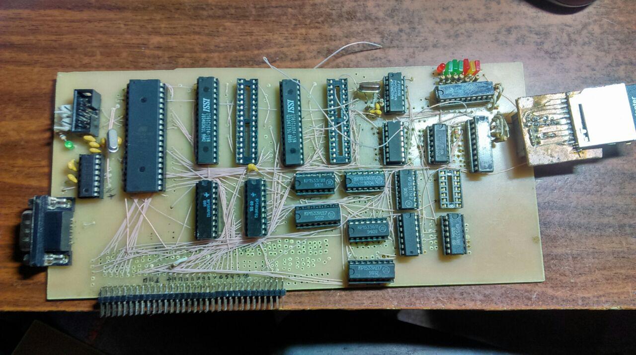
and my explanation - mostly to myself - how it works. Nothing
changed much, comparing with 8 bit scheme.
Fast clock generator is just like in 8 bit scheme. The 74HCT works mostly the same, but there are two (planned,
currently one) quarts @24Mhz. It generates /VERYFASTCLK and (should) generate /FASTCLK. And all that should be mixed
to get a (almost) real CPU clock (CPUCLK). So we have at least 3 signals and will mix them on 74151 chip.
The upper 7474 selects the clock. On reset, it clears both flipflops, setting SELCLK0 and SELCLK1 to 0,
so selecting VERYFAST to pass from pin 1 of 74151 to pin 6.
To switch to AVRCLK, CPU should access (FF)AC0000 and set both flipflops to 1, this passing pin 4 of 74151 to output.
To switch back, CPU should access (FF)AE0000. So if A1 is 0 (because the address is AE0000), both flipflops will be at 0,
selecting VERYFASTCLK, and in case of (FF)AE0002 flipflips will be set to 1 and 0, so FASTCLK will be selected.
Then, CPUCLK goes via freq divider the same manner it does on 8 bit project, and generates CPUCLK*, which goes to CPU
(pin 34 of bus connector)
Next, the SD card chematics, activated by accessing (FF)A8000. First, from the left 74138 the /A8x000 signal
is decoded on the second (right) 74138. And again, like in 8 bit project, this is done because DTACK is
almost always set to 0, with the exeption of /A90000 to /A94000 (right?) window, where DTACK signal should be
generated by a device, or BERR must raise by logic of main board.
Getting back to SD card interface, we have /A8000 signal, mix it with /OEHIGH to get /80000RD signal on the lower 7432, then
inverting it to get //8000RD active high signal on 7404 chip, and directing to 7403 pin 1. Pin 2 of 7402 is connecied to SD Card output
pin SDDATOUT, and open-collector pin 3 goes to D8 of data bus. And again, we are getting the inverted signal from SD card while
reading (FF)A8000 address on lower bit of data.
Just the same for /A8000 and /WEHI on the same 7432, /8000WR is output, inverted on 74HCT04 pin 13,12, getting 8000WR (aka
//8000WR), active high , used to latch D8-D11 on the rightmost i8282. Pins 17-19 drives the SD Card. Do not forget
that SD card is 3.3V device, so care about 7803 chip and resistors/
And after all, DTACK/BERR generator. /A90000 resets the right part of lower 7474 chip, and //A90000 (generated by 7404 pin 3,4)
sets it. So normally DTACK (active high) is set by //A90000, inverted on 7403 13+12 -> 11, getting open-collector /DTACK
(active low) and goes to CPU bus.
When /A9000 resets the right part of lower 7474, DTACK is low, /DTACK is high, so CPU is waiting something (like 68681 DUART) to
lower it. If that happens, CPU accesses memory on some different location, setting 7474 flipflop and going on. While
DTACK is high, it enables 74393 to count CPUCLK, and after it counts it, it generates BERR. BERR is inverted on 7403 to
get an open-collector /BERR signal, which goes to main CPU bus.
And, well, like that or at least very similar.

| Flag counter for 68kavr Epoch III only |