Switch to full layout
Force Russian
Main shit - the best the newest and the most realistic - all about DtZ !
:> My computers: Z80,68K, etc
:> 68008 SBC AVR (atmega8) Booted minimal computer by DtZ with serial port MC68008 :> 68K 68EC000 + atmega8 computer, epoch II - several boards and limited ISA bus
68EC000 Computer by DtZ
"Понесла'сь пизда' по ко'чкам"
Russian proverb, means "Things are up and running"
20141210
First thing to mention is a deep
satisfaction of Epoch I. I find out that I'm clever (even I suspected that), I
can do some untrivial electronics myself with an antique methods, so I could
survive when vandals occupied Roma. But if the vandals use TOS instead on CP/M 68,
they surelly sacrifice me.
The thing that warns me is my huge plans. Generally speaking, I'm limited in:
- 8 bit bus. Because I like Atmega8. Because it has 28 pins. Because
I carved out the backplane and it was hard and it has 2x29 or 2x30 pins. And because
16 bits of data bus will not fit
- The chips I can find (but there are a lot of them!)
- My soldering skills, also my technology of carving the boards with a knife.
I spend 2.5 days of carving CPU board! (Anyway, how much time was to order it? And yes, I'd surelly
made a error there, so double the time).
I can solder PLCCs and SOICs [and DIPs], but nothing more
(yes, I'm lookining at the MIPS [and other RISC] CPUs and smack my lips)
- No, I'm not going to use TinyBoot or other FORTH-powered ROM code (even I think
that's good for a good computer). Because that ROM code is ROM-oriented (well, NVRAM even).
I have few kilobytes for startup code and in multi-board setup I'm not
going to use ROMs too. The idea of AVR-booting should not end with having ROMs on expansion cards.
And well, I hate burning [E[P]]ROM or even parallel flashes (because I do it in RTL8139 NIC)
Mad idea: attach a SD card to AVR MCU(!) with the code of drivers for the CPU ;-))) (cons: I have
no legs left, but, if to think....)
So, in this project I cannot use Z8001 CPU (I have few of them) [but I can give up this project;
the best time for it is exactly after the announce of Epoch II ;-) ]. Not a Harris 6120 (even
that's VERY interesting!). So CPU's of interest are MC6809 and Z80 [I have @20Mhz parts!],
with deliveratives. I can use I8088, but it sucks and I will not touch this shit.
Anyway, MC68EC000 is the best [I mean: more advanced of them] and the most interesting for
programmer (even still I'm using 20% of it wonderful assembler command set because I'm too lazy
to read docs)
But yes, I have plans for Z80 & 6809, and that will be... Oh well, I'll tell you if it happens.
The other CPUs are not the only thing that I want to try. IDE controller should be easy [it's unclear
if I really need that, but that may be fun]. Some keyboard and video or terminal. Timer & RTC. The better serial.
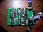
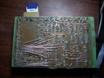
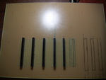
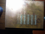
Photos of 201412.

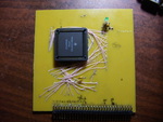
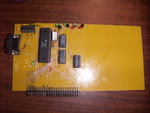
Front side with CPU
removed, 256K RAM
|

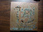
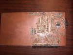
Back side.
|

Backplane front side.
|

Backplane: Back side.
|

MC68EC00 CPU Board
Front side
|

MC68EC000 CPU
Back side
|

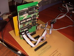
Computer ;-)
|
Video: 32M, in awful quality,
but that's all I have
20141210
So we have a SBC style computer and backplane. If we take the CPU out of SBC - I'll
call this board "System board". I'll keep compatibility with SBC for some time at least - mostly
because it's easy to test the system with this board and it will take significant time to build
a replacement one (but I'll need to - I want another [faster/more] memory chips, unground DTACK, BERR logic,
change decoder, etc)
The other board you see on the photos is the CPU board (will be discussed later in it few details).
- Not Versabus - it's very big and I've never seen any board
-
Not VMEbus - it's hard to build - 3 rows too hard to solder. (but the bus itself is very good). As I understand, some
compatible parts can be stolen from old PTSN systems. If I steal smth like that, I return to this question
-
Not S100 - it's not 68K signal native. I do not want to combine signals they just should to be at old
bus I've never seen. Again, no source to borrow S100 cards. And I do not like edge connector.
-
Not ISA - not 68k native, edge connector
-
So I build my own - as simple as possible.
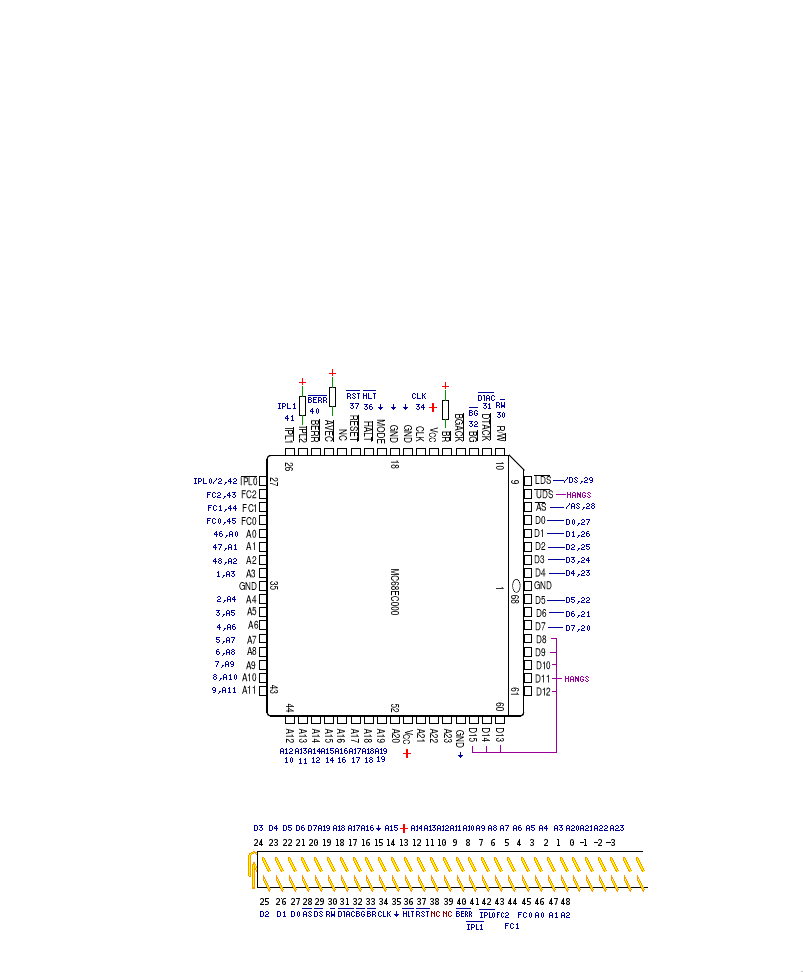
The easiest is just one pin of bus corresponds with CPU pin + several spare. So we've got (view
to the board male contacts):
       ____________________________           ______________
PIN NO [ [24] [23] [22] [21] [20] [19]  ...... [1]  [0]  [-1]
      /[  D3   D4   D5   D6   D7   A19          A3
     / [ [25] [24] [25] [26] [27] [28]         [48] [49] [50]
    |  [__D2___D1___D0___/AS__/DS__R/W_      ___A2_________
    | |
(it is also drawn in the next chapter where CPU board is shown)
Where pin No is the corresponding MC68008 pin. So that's easy to see that we have a numbers for 48 pins. And we can number the
pins in lower row future - 49, etc. The clear thing we will name pins in the other (top) row with negative numbers. After all
destroygreat innovations in computer industry made by this project that's just another sin I can afford.
The other problem that some of the sockets on my backplane are 2x30, but the others are 2x29 - I've just
did not checked them before I started soldering them. So generally that's unclear if my bus has 60 or 58 contacts. Let's say
that it is expandable by it's nature.
-
Pros: Motorola docs calls it "Embedded Controller", but it's a true CPU. It has 8 bit mode. It has more address lines.
I want them. It's in PLCC - it's hard, but possible to solder it. It's faster (I have mid-1990 10Mhz,12Mhz and ordered 20Mhz parts
[UPD: Got them (FreeScale parts of '2005), but none of the works; veeery strange]!).
It can run from 0Mhz (UPD: Wrong! Docs says there is a lower limit, and I feel my AVRClock is lower)
as I suppose it is CMOS part (anyway, I had no problems running MC68008 on low freqs).
I suppose it eats less power. It's 100% compatible. MC68SEC000 is in production still.
-
Cons: it has no VMA/VPA/E lines. I do not use them and never wanted to. It's in PLCC, and I got practice of
soldering them, so I'm not afraid of them any more. It it had virtual memory (like 010) that could be even better.
-
Alternatives: MC68HC001
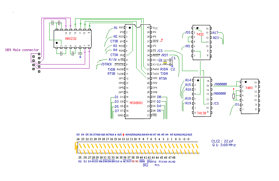
I soldered the board and it just runs. The /DS line is /LDS, MODE should be grounded and all the inputs should be pulled up!

20150114 I'm from Z80 world and in the first moment DTACK confused me, but next I thought about
it as WAIT signal with different polarity, grounded it and forgot about it. Really I was very
happy without it till the moment I decided to try 68681 DUART chip, because I have them (I ordered them before I
decided to use AVR based UART). And because they may give me not only 2 extra serial ports (and the
good computer must have a lot ot serial ports), but there is timer! Timer! Timer!
And because now I have a backplane and not limited to the breadboard space.
Timer can give some real-time processing. Saying if anyone is able to find how to port CDOS
(Concurrent CP/M) , that will give multitasking. I do not know if TOS wants it, but I do.
So the first thing is DTACK & BERR. DTACK was always grounded, and it will be mostly-always
grounded - but we'll have a small window in address space which will require to generate and external
real DTACK.
Also, thing to mention - 68681 is the only DTACK genetating device I know I may want.
So for keeping compatibility the 90000 - 93FFF space was selected for this window. Sure,
the extra 138 chip will decode /A80000 line (which from now on will be called /A8XXXX; do not
forget to rewite SD card interface from /A8XXXX to the new /A80000) and /A90000 line
should clear the trigger. The thing that should set this trigger is, after several tries, was chosen
just an inverted //A90000 line. Then DTACK should be transformed to open collector output and that is
done by - what else - 7403.
The BERR signal should happen when DTACK is active for some long time. Anything long
time is - we need a counter, and that's 74393, which will set it's X16 output up in 8 clicks
of ... what? Hm, saying, CPUCLK, the slow clock generated by AVR. I said that I think that
it is hundred times slower then main clock, FASTCLK, no matter if FASTCLK is 4 or 12 Mhz ;-).
Anyway, 8 ticks of that is a relatively long time (at least, as practice shows, enough for 68681; anyway,
we have the other half of 393). And we'll invert it and lead directly to /BERR input of CPU.
At least accessing this space on running CP/M says "Exeption #2" (or like that), that means
that it really thinks BERR happened (but the firmware does not - I currently hanlde it wrong).
20150211

From the hardware point, "Just solder it". (and pull up all inputs)
Some notes:
- The four leds are RX TX (lights on zero) RTS CTS (lights on logical 1)
- It should be on $90000-$93FFF (aka $FF790000) because of DTACK and BERR stuff mentioned in ch.III
- Interrupts are still not used because I've just got 74148 chips
- This funny 7403 on D1 bit of SDPORT ($80000 [aka $FF780000]) acts as software detector that card is present
From the software point of view, that's a time
- To write a tiny terminal program to ensure it is working with, saying, real RS232 modem
- To implement a IOBYTE and play with that nice
STAT CON:=CRT:
20150202
Here is a terminal program
20150622
In the 2560 release, the BIOS knows about 68681, and even understands 7403:6 detection of the presence
of the card (bit 1 of $80000 port [really it checks $FF780000 ; know why by reading the following chapter
about ISA adressing]).
IOBYTE is semi-supported: if IOBYTE is not 0, console is redirected to port 1 of DUART; you may get it
by making STAT CON:=TTY: and back by STAT CON:=something else.
And it is accessable as UC1: or UR1: or smth like that.
(Check it when I turn it on the next time)
It's known to contain some bugs: while it sets the speed to 38400 and works with strict RTS/CTS, it has,
as serial on AVR did before 2560 release, an error understanding when remote asks to pause the transmission,
so it's a superb-fast console (when it is redirected there by STAT; the firmware does now know about
68681 serial at all) (but kermit transfers are not possible because of the mentioned bug)
At 9600 (change the speed by tuning BIOS) on my setup RTS/CTS was not activated during
kermit file transfers, so I can say that it outperforms AVRSerial even 68681 runs at 9600 and AVRSerial @ 38400
And this is not the end of this chapter; I want to fix this nasty bug and make use of IRQs.
20150626 That should be move to the Epoch III,BTW

(UPD 201902: ALE line shown)
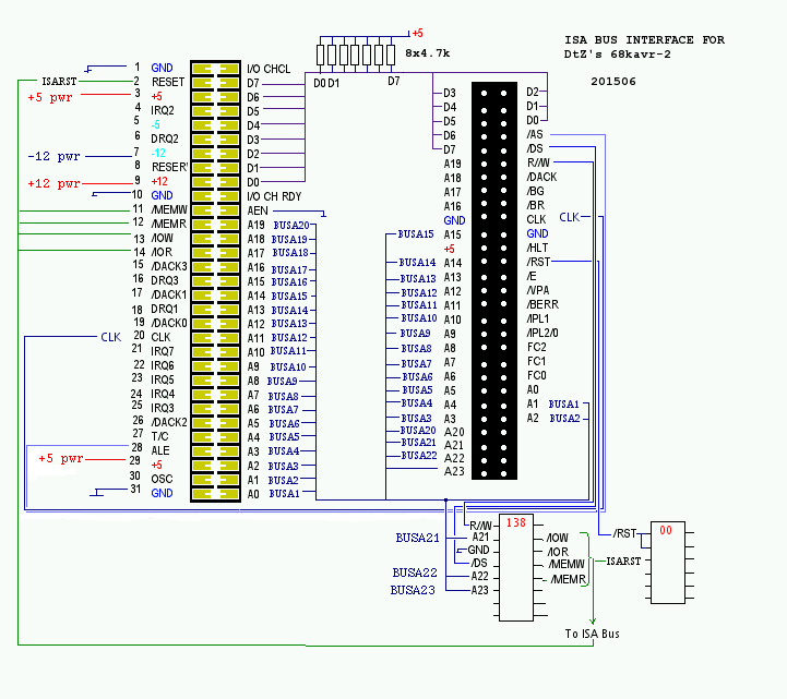
And here the ISA bus (really,some subset of it: no IRQs [planned], no DMA [not planned]).
Things to tell about it: for accessing ISA IO and ISA Adress Space
we need to select two 1M windows, but, because I think about future migrating to 16 bit central
card, I will not use A0 line, so I need two 2M windows (yes, I can use less space, but I have a lot of
adress legs). , and we select A23=1,A22=0 to access ISA,
A21 = 0 for ISA IO space and A21 = 1 for ISA memory
That is why on the main board U4:5 input of the 138 decoder shoud be disconnected from /AS and
connected to A23 (generally there should be a jumper to keep backward compatibility with 68008 without A23 line)
The DUART is not affected,because it already mentions A23=0 at 7432:12
That leads to the following address map changes:
- Memory from 0 to the end of 512K
- All onboard devices (AVR Uart,clock switcher,SD card) and DUART should be accessed as FF7xXXXX (bit 23=0)
- To access ISA port 3XX, we should get a pointer to
FF800000 + (3XX<<1) + 1
- To access ISA adress XXXX, we should get a pointer to
FFA00000 + (XXXX<<1) + 1
(and this is the subject of change; anyway the current system, 2560, is backward compatible with the early 68008
system)
&nsbp; A +1 in this formulas is a workaround for 16-bit bus.<>
Release 2560 knows about that adressing tricks, you should update both system (CPM.SYS and CPMLDR)
and firmware.
Also, mind that ISA hardware may be slow and you should switch clock slow, then access ISA bus, then
switch clock to full speed (but till now I access all the ISA devices at full speed on my 12.5Mhz CPU clock;
I was really thinking about the third system clock, around 4.77/5 Mhz)
Also, get an ATX power supply and feed all the computer with a lot of power (you need +12 -12 for
yours ISA cards anyway)
Just for curiosity: I have all the 8250/16550 cards working, including ISA modems and VLB card
(yes, in 8 bit ISA slot, and only thing I've tried was COM port) (I've not tried IRQs (for sure),
RTS/CTS, Fifo, etc, and the max speed without loss of bytes was 1200) and I've got a video out
of MDA card (on MDA monitor)
Next thing to be published is some example code.
And yes - edge connector is piece of shit!

| Flag counter for 68kavr Epoch II only |
