|
1802 computer (1802avr) by DtZ
It has SEX ( E0 - EF )
Preface
Well. I've never programmed CDP1802. I have 4 pcs of this chip. I have huge practice with
AVR-booted 68008 & 68x000 chips. I'll solder it!
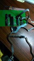
Board fotos:
| 201712 | |
|
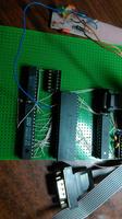
|
20171219
It's winter again and I want to solder some other computer. I did not gave up working with Z80/68k family, no. I just
want to solder one more computer. And I want it to be weird. The weirdest CPU I could get (and get enough info for that)
is 1802.
But well - that's a weird CPU, but the design of a board is very classic for this CPU. While the CPU, speaking about
it interfacing, looks like a 8 bit CPU with multiplexed adress bus, it has a very specific DMA feature. In short, you are
able to load it via front panel! Just like, saying, PDP-8! Means, you trigger 8 mechanical switches, press a key "Eat it!",
and the byte goes to memory!
Sure that will be an AVR chip - again, ATMega8 - which will boot it. Panel is GOOD, bit it's hard to build, and, well,
I'll not use it more then once.
So that will not be any risky investigation which were made while booting 68008 in Stage I of the
68kavr project, that's a documented way to load it.
So the initial scheme is:

First thing to be said, the project shares mostly everything from a Stage I of 68K project .
Look at Atmega8. AVRISP is AVRISP socket. RS232 header and MAX232 are, well, RS232 header and MAX232. Currently RTS/CTS are
not used. And quartz on AVR pins 9 and 10 is missing. Several pins goes to data bus. And a strange lines named /DMAIN, /DMAOUT,
/WAIT, and SC1. And a classic lines CPUCLK (yes, ATmega clicks Clock for CPU) and CPURESET. Those to be discussed.
CPU, just CPU. Because it has a multiplexed address bus, I have to unmultiplex it. And that's what 74LS373 does. Well, I know
CMOS parts are preferred, but this classic TTL chip still works. It should latch A8-A15 on raise of TPA and it really does it.
RAM, just RAM. On your's choice. Some static RAM. I'll talk about it later, but, well, it's just RAM.
CPU has Q PIN4. That's a programmable CPU output. You can set it to 1 (SEQ command) and to 0
(REQ). And the first thing I'll do is blinking it.
One of the strange thing that CPU does - it sets several outputs to 0 when you expect
them to be at high impedance! If you reset it, it keeps address but
at 0! So it does with Q output.
So, from the docs, I should deal with /CLEAR and /WAIT lines. /CLEAR is much like /RESET; /WAIT is much like Do-nothing signal.
On both /RESET and /WAIT CPU clears its' registers and starts to do nothing.
There is /DMAIN (DMA IN) signal, which causes CPU to pick up a byte from data bus, put it to the memory address pointed
by some 16-bit register, and increment it. After eating a byte CPU sets SC1 line, so I disactivate /DMAIN, and go to next iteration.
So first I will reset CPU, click several clicks (I have a lot of clicks to click, so let there be some) and start
loading bytes in CPU.
Here is how:
- RESET (aka CLEAR) down
- Click 1200 times
- WAIT down
-
Writing byte
- Put next byte on data bus
- DMA IN down
- Click Clocks and wait SC1 to get low, this way CPU says it started DMA cycle
- DMA IN up
- Click Clocks and wait SC1 to get high, this was CPU says it ended DMA cycle
- Get byte off the data bus and free it
- Repeat till I have bytes to load
- WAIT up (still having RESET down)
- Click 1200 times
- Raise RESET
- Watch Q signal - it should be blinking because of program I load there
And here is the program:
0x7A      SEQ
0x7B      REQ
0x30 0x00 BR 00
Clear, right?
It took me two weeks to figure that out - and guys from Yahoo!
Cosmac Elf group (yes,
the CPU is weird itself and it has a group on Yahoo!) helped me a lot because 1802
has a strange memory read algorytm.
But I'll tell you sometimes later.
And here is the code . gcc for avr will compile it.
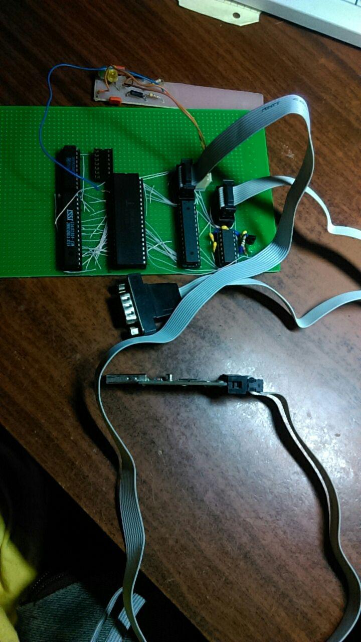
20171227 The updated scheme.

And well, I will use AVR as UART - as I always did. 1802 has a dedicated pins for adressing of IO devices.
That has some very specific logic - the OUT and INP commands writes and reads byte from memory to IO devices during
normal cycle, raising TPB active high and showing 1-7 (but never 0) on N0-N3 pins. The input and output
is determied by /MRD signal and not by /MWR. During OUT, CPU reads from memory with /MRD and writes it to
devices with TPB, keeping /MRD active, direcly from memory. During INP, CPU activates /MWR, this allowing write
to memory, and wants data came out the device on TPB from device directly to memory, too.
In this project, I will not use quartz for CPU. In 68K I could run CPU on 12Mhz or even higher, but for
1802 I'm limited sort of 2,5Mhz, so AVR clock looks fine, if to run AVR from 16Mhz or like that. Normally
I should look at the assembler code generated by AVR C compiler and count freq.
So, I'll deal with UART inside of main loop in AVR, not with interrupts as in 68kavr Stage 1.
The OUT command is tricky as hell (and as every command of 1802)
It looks like
OUT 1
It outputs to port 1, this setting N0 N1 N2 to 1 0 0 and writes there, as said, from memory. The memory
location is specified by one of the 16 bit registers (and it is incremented by OUT command!). The exact register is the one selected by
SEX 5
command. And the register must have some value. In Z80 world, it's ok to write
LD HL,$BABA
, in 68k,
MOVE.L #$BABAEBBA,A0
, but 1802 use a different approach, very similar to RISC CPUS.
It can load 8 bit value to accumulator, then set lower half of 16 bit register, then
load another part of value to 8 bit accumulator, then set higher part of 16 bit register.
That looks like
    LDI HIGH TEXT ; high part of address of TEXT goes to acc
    PHI 4	  ; acc goes to higher part of R4
    LDI LOW TEXT  ; low part of address of TEXT goes to acc
    PLO 4	  ; and to lower part of R4, so R4 now contains TEXT address
    SEX 4	  ; we'll have sex with R4, meaning R4 will be used as register for OUT and INP
START:	LDN 4	; (R4) -> acc, for comparing, if it is zero or not
    BZ	ENDLOOP	; if it's zero, give up
    OUT 1	; write (R4) -> port 1
    BNZ	START	; Well, OUT also increments R4!
ENDLOOP:	; and blink Q forever
    SEQ
    REQ
    BR ENDLOOP
TEXT:	DB "Fuck a duck!\n\r",0
    END

| Flag counter for 1802avr |
|
